Section 53.5 Band Structure
We have seen in previous section that we can understand several aspects of electric and heat conduction of metals by modeling metals as free electrons, whether as a classical gas or as a quantum gas. This begs the question: What is the role of the core of the atoms in a metal? Since ignoring the complications from the electron-electron repulsion has led us to some stunning results already, we would continue to treat the conduction electrons as independent of each other and only attracted to the cores by the Coulomb force. Modeling the metal as a perfect crystal without impurities or defects will also simplify the problem. Then, the answer to the question of the role of the nucleus of a metal atom should be present in the solution of the Schrödinger equation of an electron moving in a periodic potential \(U(\vec r)\text{.}\)
\begin{equation}
-\frac{\hbar^2}{2m}\left[ \frac{\partial^2 \psi}{\partial x^2} + \frac{\partial^2 \psi}{\partial y^2} + \frac{\partial^2 \psi}{\partial z^2} \right] + U(\vec r) \psi = E \psi , \tag{53.16}
\end{equation}
with
\begin{equation*}
U(\vec r +\vec R) = U(\vec r),
\end{equation*}
where \(\vec R\) is a vector connecting any two points in the lattice, reflecting the periodicity of the lattice. In 1928 Felix Block proved that the wave function of an electron in a periodic potential will have a particular form, called the Block wave form, in which a periodic wave \(u(\vec r)\) is modulated by a plane wave of wavelength \(\lambda = 2\pi/|\vec k|\text{.}\)
\begin{equation*}
\psi(\vec r) = e^{i\vec k \cdot \vec r} u(\vec r),
\end{equation*}
where \(u(\vec r)\) is a periodic function with the period of the lattice,
\begin{equation*}
u(\vec r +\vec R) = u(\vec r),
\end{equation*}
and \(\vec k\) has units of inverse length or wave number. Using vector \(\vec k\) we define the crystal momentum, \(\vec p\text{,}\) by
\begin{equation*}
\vec p = \hbar \vec k.
\end{equation*}
Note the vector \(\vec p\) is not the momentum of crystal, but instead it is a momentum associated with the electron wave. When you insert the Block form in Eq. (53.16) you obtain a complicated equation for \(u(\vec r)\) which can be solved for simple examples of the periodic potential \(U(\vec r)\text{.}\) There are infinitely many solutions for each value of \(\vec k\text{.}\) We label these solutions by an integer \(n\text{,}\) called the band index. Thus, the wave function of an electron in a periodic lattice is characterized by a wave number vector \(\vec k\) and an integer \(n\text{,}\) and the same goes for the energy \(E_{\vec k, n}\text{.}\)
\begin{equation*}
\textrm{Solutions:}\ \ \psi_{\vec k, n}(\vec r) \ \textrm{corresponding to energy} \ E_{\vec k, n}.
\end{equation*}
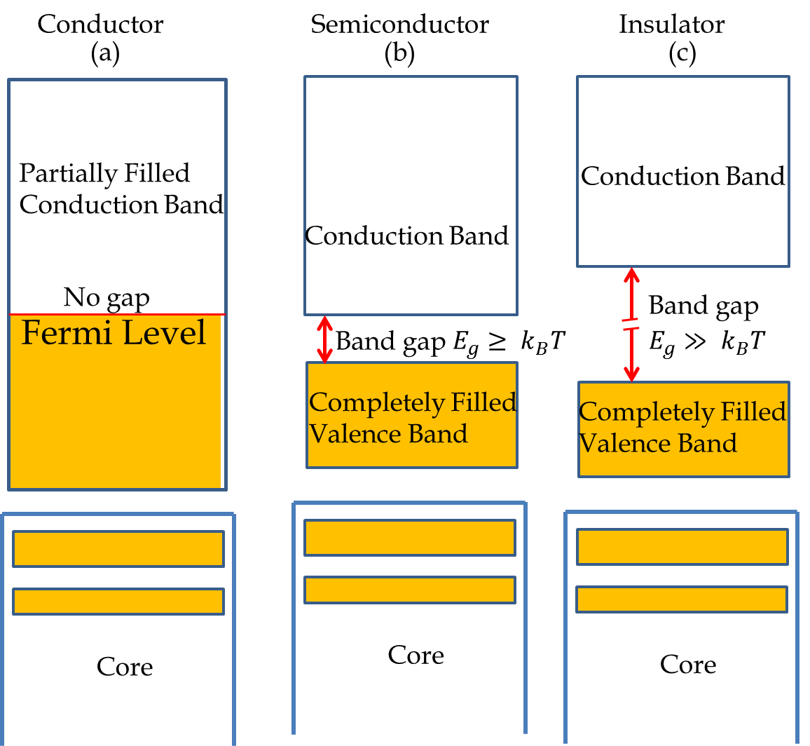
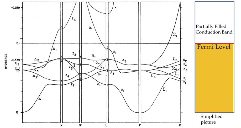
A plot of the energy \(E_{\vec k, n}\) for different \(n\) versus \(\vec k\) for copper are shown in Figure 53.20. In these diagrams the values of \(k\) are plotted towards various directions of \(\vec k\) in the \(\vec k\)-space. The diagram shows continuous bands of allowed energy values. Although some bands have gaps at some values of \(k\text{,}\) but there is no gap here if every direction of \(\vec k\) is taken into account: there is at least one state at all energies. Therefore, as you fill electrons in these energy levels, the electrons have continuous energy up to the bands labeled \(\Delta_1\text{,}\) \(Q_{-}\text{,}\) and \(\Sigma_1\text{,}\) which are not fully filled by conduction electrons. The unfilled band at the Fermi energy is a hallmark of metals - actually, we take this to be the electronic definition of a conductor. If the band is partially filled, as is the case here, there are states available to the conduction electrons within an infinitesimally small energy range of the highest filled state, which makes conduction possible with the slightest push.
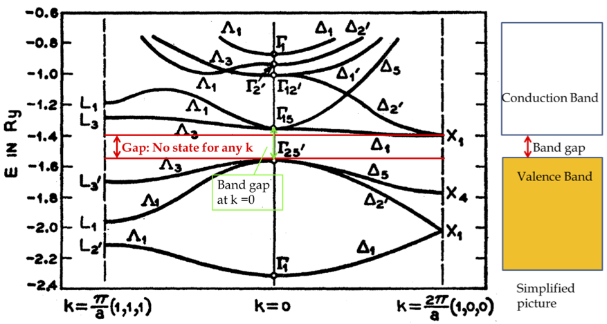
The band structure of copper should be compared with that of a semiconductor such as silicon whose band structure is given in Figure 53.21. The band at the Fermi level of silicon is completely filled with a gap in energy before the next energy states are possible. If there is enough thermal energy \(k_BT\) or photon energy \(hf\) from an incident photon is supplied to the electrons of the filled band, some of the electrons will move to the next level, which will cause two partially filled levels, one upper level and the other the lower level. The excitation is necessary to cause Si to conduct electricity. The lower band is called the valence band and the upper level the conduction band. The energy gap between the two bands is called the band gap.
Continuing in the spirit of band structure of materials, if we analyze the band structure of diamond, which is a good insulator, we find that the bands of carbon in the diamond structure are similar to the bands of silicon, which is not a surprise since both are Group IV elements in the periodic table and both have the same lattice structure. However, the band gap in diamond is 5.5 eV, which is much larger than the band gap of 1.1 eV in silicon. The energy gap in diamond is almost 200 times the thermal energy 0.026 eV at room temperature, \(T = 300\) K. The probability that an electron from the valence band will be excited to the conduction band thermally can be calculated from the Fermi level and the energy of the final state.
\begin{equation*}
f_{\textrm{FD}} = \frac{1}{e^{(E-E_F)/k_BT} + 1}.
\end{equation*}
To perform this calculation, we need to know \(E_F\) in the case where the valence band is completely filled. Note that, in this case, the energy required to remove an electron will be equal to the the binding energy of the top of the valence band; on the other hand, when you want to add an electron you cannot add it to the valence band, instead you will need to place the electron in the conduction band - to add an electron, we need to extract only the energy corresponding to the bottom of the conduction band. Therefore, we place the Fermi level in the middle of the gap. Therefore, \(E_F\) will be taken to be
\begin{equation*}
E_F = E_V + E_g/2,
\end{equation*}
where \(E_V\) is the energy of the top of the valence band and \(E_g\) the gap. With \(E=E_C\text{,}\) the energy of the bottom of the conduction band, after simplification, we get the following probability
\begin{equation*}
f_{\textrm{FD}} = \frac{1}{e^{( E_g)/2k_BT} + 1}.
\end{equation*}
Now, putting in the numbers we get the probability to be
\begin{equation*}
f_{\textrm{FD}} = \frac{1}{e^{5.5\:\textrm{eV}/(2\times 0.026\:\textrm{eV})} + 1} = 1.2 \times 10^{-46}
\end{equation*}
This makes it extremely unlikely that any electron in diamond will be in the conduction band. That is why diamond is a good conductor. Figure 53.22 illustrates the essential difference between a conductor, a semiconductor, and an insulator.