Section 53.6 Semiconductors
Subsection 53.6.1 Electron and Hole Carriers
We have seen above that the band structure of a semiconductor is such that there is an energy gap \(E_g\) between the highest filled band (the valence band) and the next empty band (the conduction band) which is not too large compared to the thermal energy \(k_BT\) available at that temperature \(T\text{.}\) As a result of thermal energy some of the electrons from the valence band are excited to the conduction band. However, the density of conduction electrons in silicon at room temperature \((T = 300 K)\) is in the range \(10^{10}\) per \(\text{cm}^3\text{,}\) which is far cry from \(\sim 10^{28}\) per \(\text{cm}^3\) in a metal.
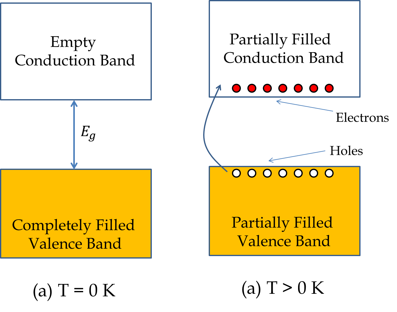
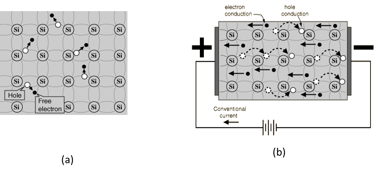
In a semiconductor without doping, such as a pure Si crystal, the valence band has as many empty states are there are filled states in the conduction band since the electrons in the conduction band come from the electrons which were in the valance band before excitation. That is, for each electron that moves to the conduction band, a hole opens up in the valence band. A hole is an unoccupied state in the valence band. As a result, both the conduction band and the valence band are partially filled states as illustrated in Figure 53.23, and electrons in both these bands contribute to the conduction as illustrated in Figure 53.24.
Subsection 53.6.2 Doped Semiconductors
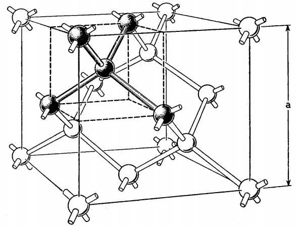
Pure silicon (Si) crystal forms a diamond crystal lattice in which each Si atom is covalently bonded to four other Si atoms as shown in Figure 53.25. Each Si atom has four valence electrons, each of which is shared with other Si atoms. Thus, there are eight elctrons around each Si atom. The sharing of electrons between Si atoms competes the atomic shell for each Si atom.
Now, suppose you replace some of the Si atoms by Arsenic (As) atoms, which have five valence electrons. Arsenic atoms will make four bonds with four Si atoms around it and will have one left over valence electron which will act as a conduction electron. Therefore, introducing As impurities in Si will introduce conduction electrons in the material. In these materials there will be more (conduction) electrons than holes as illustrated in Figure 53.26(a). When you apply a voltage across these materials, the electricity is conducted by both the conduction electrons and the valence holes, however, more current is carried by electrons than by holes. Therefore, we say that in As-doped Si electrons are majority carriers and holes are the minority carriers.
The semiconductor in which a Periodic Table Group IV element is doped with a Group V element is called \(n\)-type semiconductor with the letter \(n\) denoting the majority carrier being (negatively charged) electrons. The atom with the extra electron, here As, is called the donor atom.
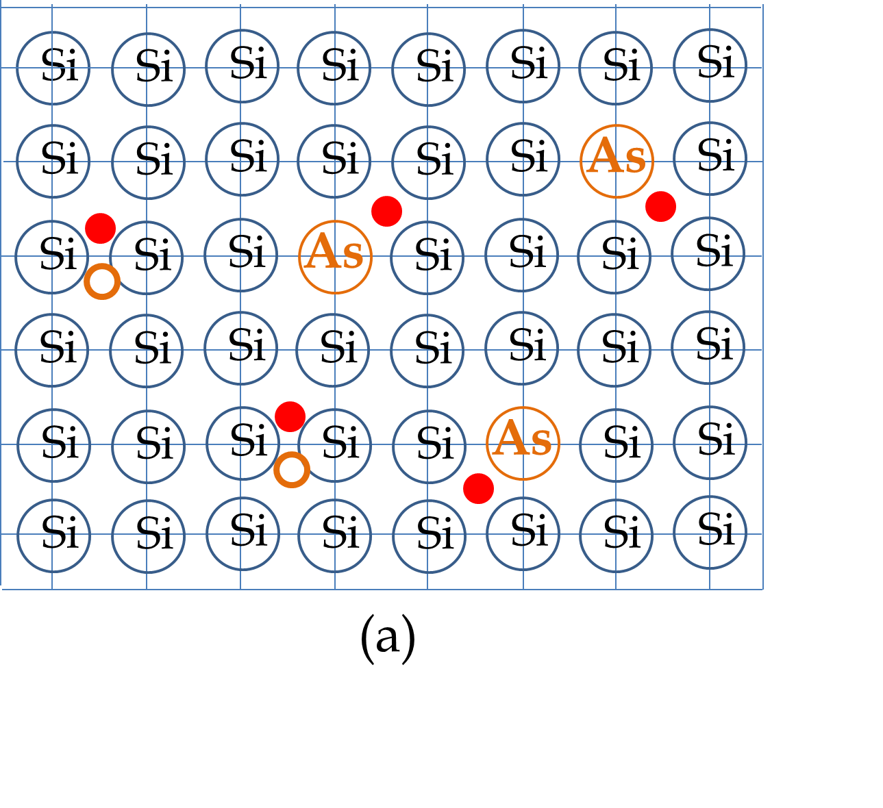
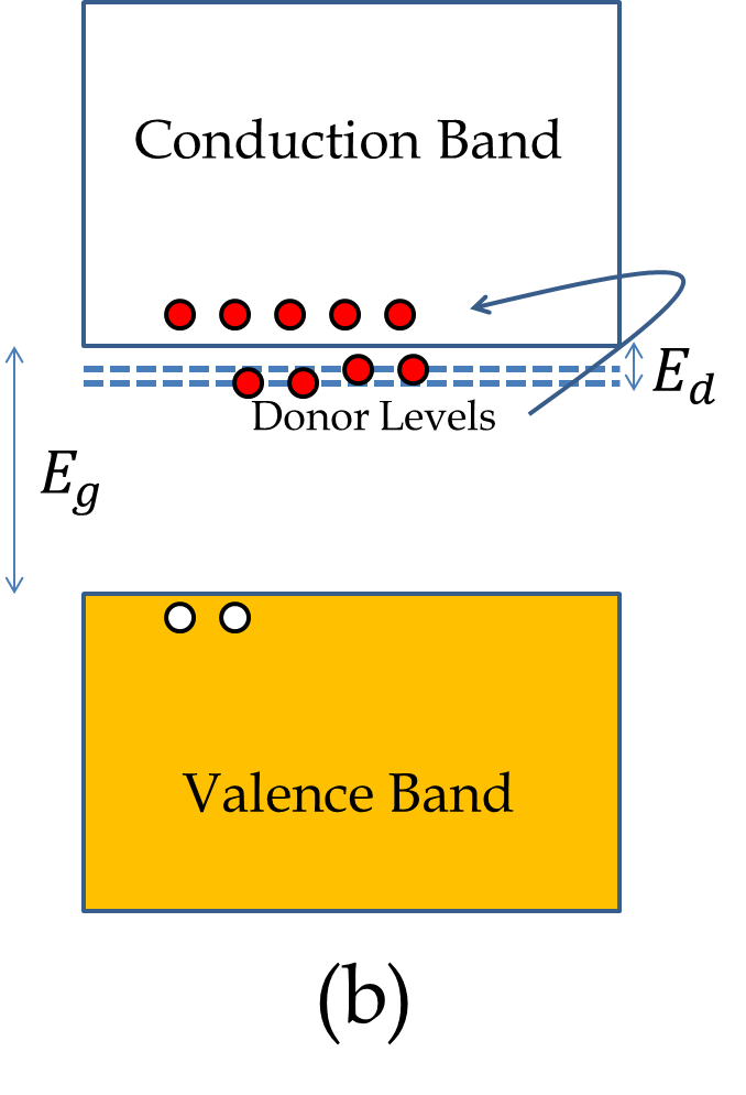
We can understand the transfer of electron from the donor atom to the lattice by noting that due to shielding of the core electrons, Si acts as a net +4 nucleus with 4 electrons around it and As as a net +5 nucleus with 5 electrons. When four electrons of As are paired with the four electrons of Si, the As site is like a hydrogen atom with net charge +1 at the nucleus and one electron loosely bound to it. Solving the H-atom problem for this quasi-hydrogen atom we find that the energy of this electron is in the band gap of the host lattice of Si just below the conduction band of the Si lattice as illustrated in Figure 53.26(b). The electrons in the donor levels are easily excited to the conduction band.
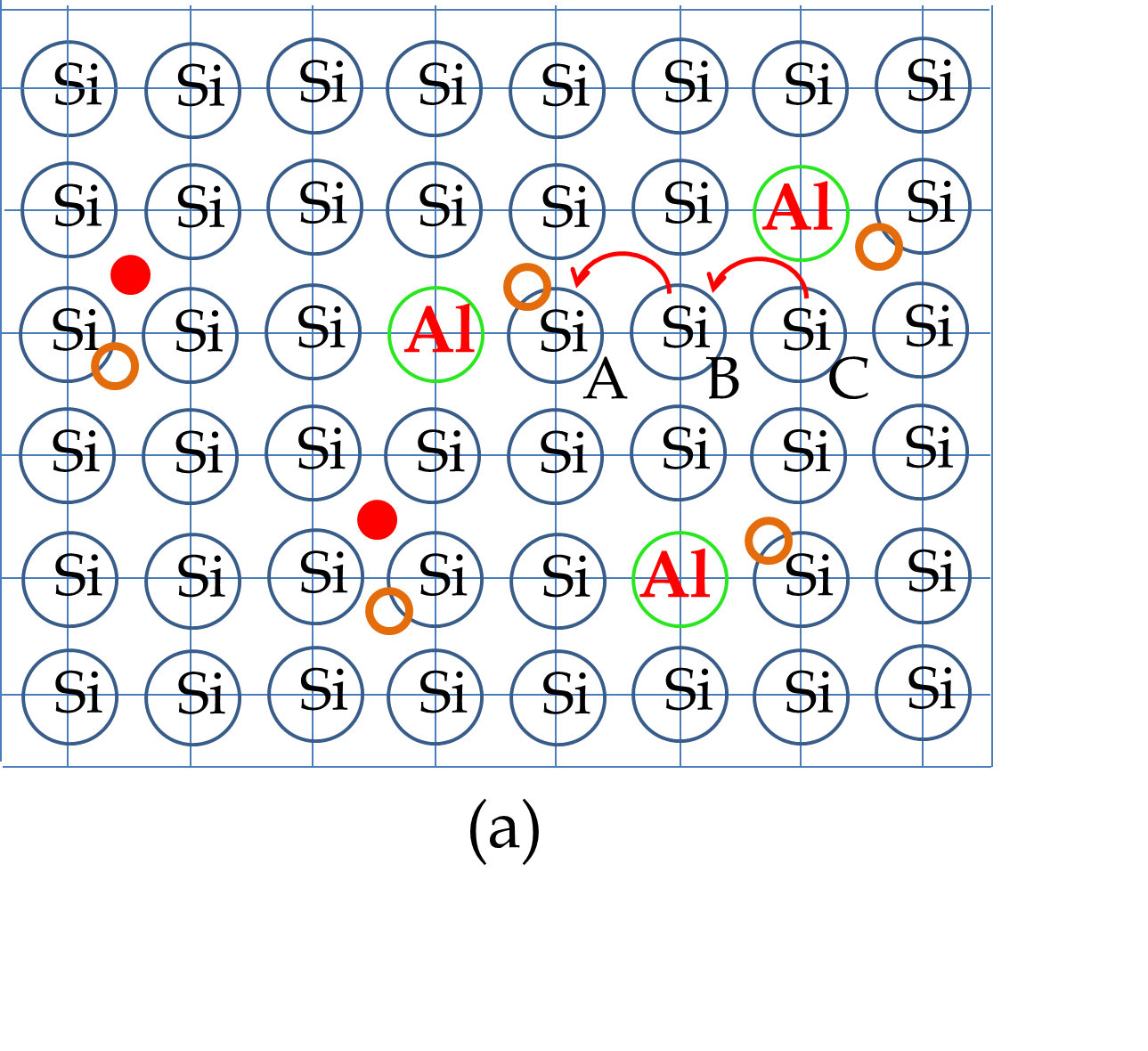
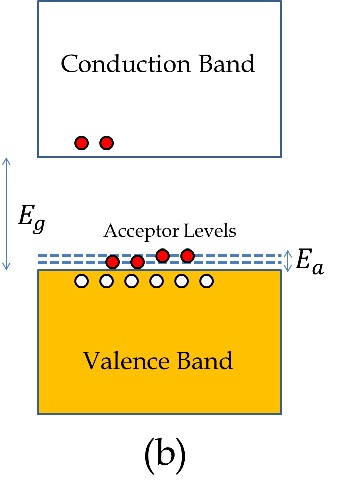
Group III elements such as Aluminum (Al) have only three valence electrons. Therefore, when you dope Si (Gourp IV element) with Al, there is not enough electrons to share to complete every atom’s atomic shell. Consequently, the valence band will not fill up as was the case with pure Si. As we have seen before, the unfilled states in the valence band act as holes in the valence band. The electrons from the neighboring atoms fall in the hole, and in this way, the hole is transferred to the next atom, giving rise to the motion of the hole in the system, as illustrated in Figure 53.27(a). The conduction by holes is distinct from the conduction by electrons - while the conduction by electrons occurs in the conduction band, the conduction by holes occurs in the valence band.
The energy levels of the acceptor atoms are close to the top of the valence band of the host crystal which makes it easy for an electron from the valence band of Si to jump to the empty acceptor quantum state, in the process creating a hole in the valence band, as illustrated in Figure 53.27(b). The current in this type of semiconductor is mostly carried by the mechanism of hole motion rather than electron motion. The semiconductor of this type is called \(p\)-type, where the letter \(p\) indicates positive carriers, since holes, being absence of electrons, act as positively charge particles.
Subsection 53.6.3 The p-n Junction
What will happen if you bring a \(p\)-type semiconductor in contact with an \(n\)-type semiconductor? Let us consider the concrete example of Si/Al as \(p\)-type and Si/As as \(n\)-type. Initially, near the junction there will be conduction electrons on the \(n\)-side and holes (empty states) on the \(p\)-side. Therefore, conduction electrons will simply flow from the \(n\)-side to the \(p\)-side, creating a region free of mobile electrons and holes as shown in Figure 53.28 This region is called the depletion region. A depletion region could be hundreds of microns wide.
The flow of conduction electrons from the \(n\)-side leaves the donor atoms with an extra proton, making the \(n\)-side near the junction become positively charged. At the same time, the flow of electrons into the holes on the \(p\)-side makes the acceptor atoms negatively charged, causing the \(p\)-side of the junction become negatively charged near the junction. The charged regions create an electric field in the direction \(n\) to \(p\text{,}\) which opposes the motion of electrons across the junction. At equilibrium the flow of electrons stops with a potential difference across the depletion region as shown in Figure 53.28. The potential developed is called the intrinsic voltage, \(V_i\text{,}\) which is positive on the \(n\)-side and negative on the \(p\)-side.
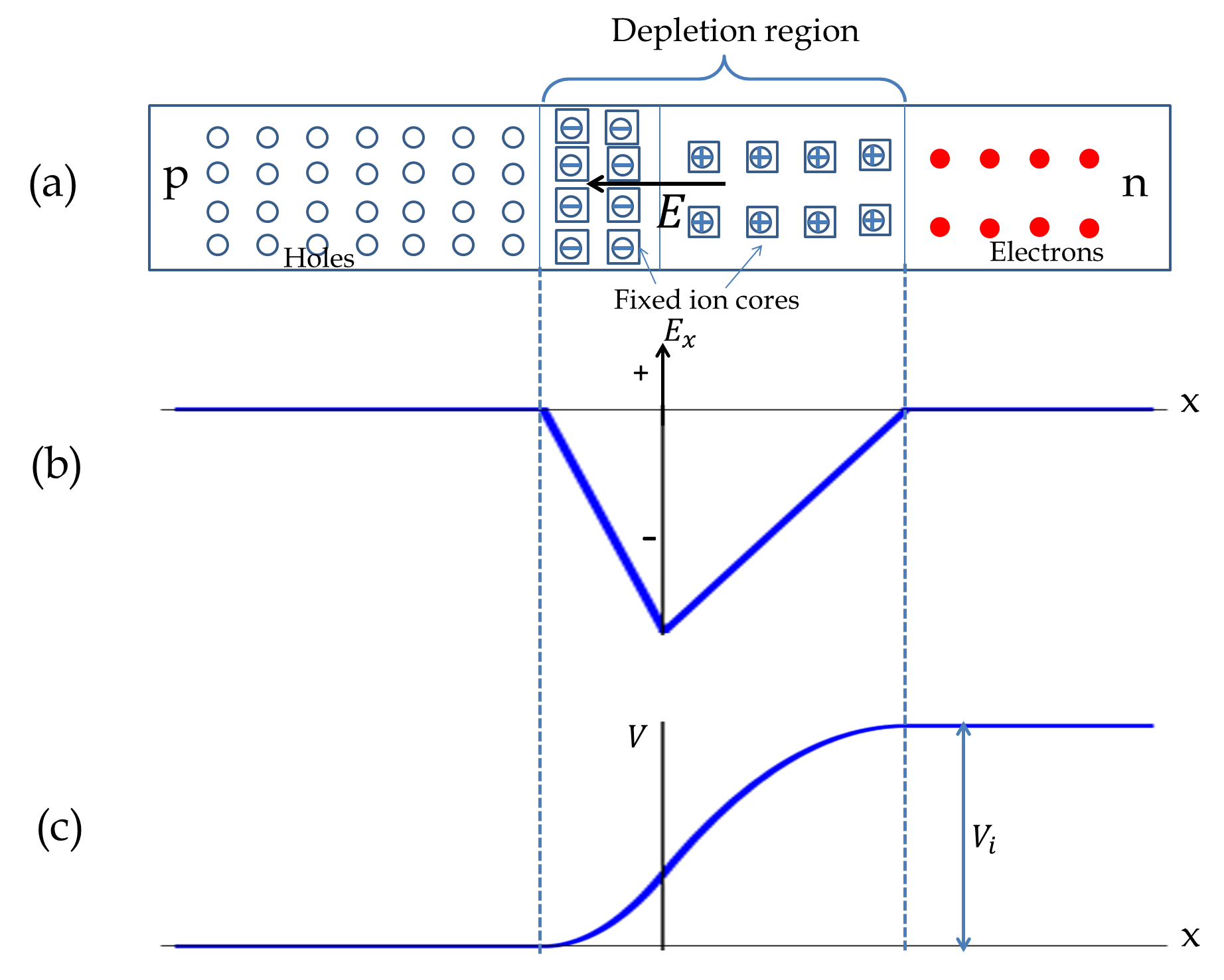
Note that although the \(p\) region has more holes than conduction electrons, it still contains conduction electrons. The built-in electric field opposes the diffusive flows of the majority carrier, thus bringing a stop to their flow at equilibrium. Because the majority and minority carriers are oppositely charged, the built-in electric field actually accelerates the minority carriers. So, any minority carrier that makes it in the depletion region is quickly swept away to the other side of the depletion region.
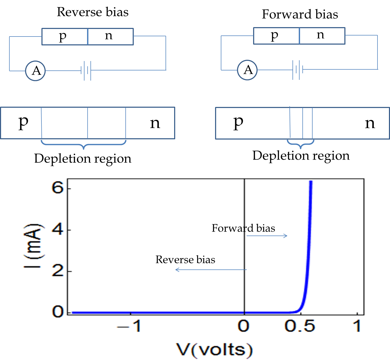
A \(pn\)-junction responds to an external voltage in a very interesting way: the current depends on the polarity of the connection. If the \(p\)-side is connected to the negative side of a voltage source and the \(n\)-side to the positive side, the so-called reverse-bias connection, there is hardly any current - current may be picoAmp or less. But, if you connect the other way, the \(p\)-side to the positive of the voltage source and the \(n\)-side to the negative, the so-called forward-bias, a large current flows as shown in Figure 53.29. In this way, a \(pn\)-junction is like a one-way electronic valve. If you connect an AC -source to the \(pn\)-device, the output signal will be rectified with only half the cycle passing through the \(pn\)-junction. The circuit element that uses \(pn\)-juction is called a diode.
Subsection 53.6.4 The Light-Emitting Diode
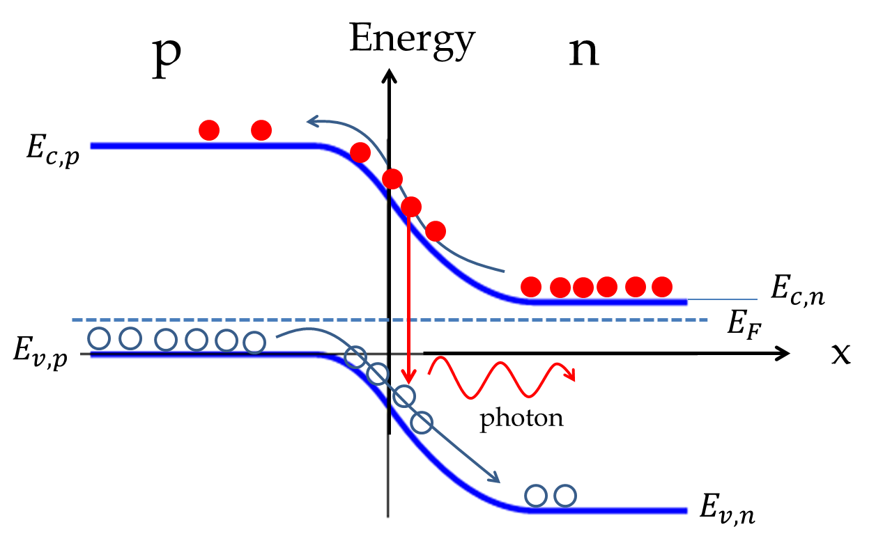
If a \(pn\)-junction of two highly doped materials is driven with a strong forward bias, the majority carriers from both \(p\) and \(n\) are injected into the junction region. The electrons then fall into hole states in the junction region. This is similar to the de-excitation of an electron from a higher energy state to a lower energy state. In the light-emitting diode the difference in energy is given off as light. From energy conservation, the energy of the released photon will equal the gap energy \(E_g\text{.}\)
\begin{equation*}
hf = E_g
\end{equation*}
By adjusting chemical content of the \(p\) and \(n\) materials one can design diodes that emit light in visible range.
Subsection 53.6.5 The Diode Laser
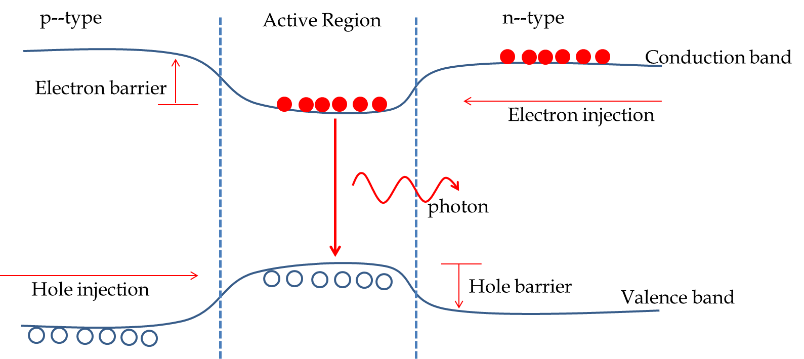
The diode laser is based on the principle that when you inject electrons from the \(n\)-side and holes from the \(p\)-side of a \(pn\)-junction, there is population inversion with higher quantum states occupied and lower states unoccupied. Laser diode is made possible by sandwiching a material between the \(p\) and \(n\) material that has a narrower band gap than those of the \(n\)-side or \(p\)-side so that the injected electrons and holes become trapped in the active layer and can combine to produce photons. The continuous pumping of the electrons and holes into the active region acts as the pump for the laser. These lasers are also called injection-pumped lasers due to the mechanism by which they are pumped.
The original diode laser was based on the GaAs as active layer sandwiched between an \(n\)-type GaAlAs and a \(p\)-type GaAlAs. Current is injected into the structure by connecting it to a current source with positive voltage connected to the \(p\)-end and the negative voltage at the \(n\)-end. The energetics and injections of majority carriers are shown in Figure 53.31.
\begin{exercise} The energy gap in the Germanium is 0.67 eV. (a) What will be the longest wavelength of the photon that can excite an electron from the valence band to the conduction band? (b) What will happen if you expose a sample of Germanium to a light of longer wavelength? (c) What will happen if you expose a sample of Germanium to a light of shorter wavelength? \end{exercise}
\begin{exercise} Often the band gap in a semiconductor is measured by absorption spectrum. It is found that the longest wavelength that a semiconductor will absorb is 1.1 $\mu$m. What is the band gap? \end{exercise}
\begin{exercise} Silicon has a band gap of 1.14 eV. If the Fermi level is taken to be halfway between the Conduction and Valence bands, what is the probability that a state at the bottom of the conduction band will be occupied at (a) T=250 K, (b) T=300 K, (c) 350 K? \end{exercise}
